
Polyimide (PI) films are indispensable in advanced manufacturing, prized for their exceptional thermal stability (withstanding up to 400°C), mechanical strength, and electrical insulation properties. Widely used in flexible electronics (e.g., OLED displays, flexible PCBs), aerospace insulation, and high-temperature adhesives, even minor surface defects can compromise their performance. Defects such as scratches, pinholes, wrinkles, foreign particles, or coating inconsistencies threaten reliability in mission-critical applications. This article explores the specialized technologies addressing the unique challenges of PI film surface defect detection.
1. Unique Challenges of PI Film Inspection
PI films present distinct characteristics that demand precision detection:
Transparency & High Surface Smoothness: Light reflection and low defect contrast make subtle flaws (e.g., 10-50 micron pinholes) hard to identify.
Thin Gauge & Complex Geometry: Films as thin as 5 microns in flexible electronics require sub-micron resolution, while curved or layered structures (e.g., folded OLED substrates) complicate uniform imaging.
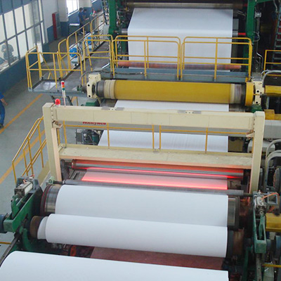
High-Temperature Production Environments: PI films are often processed at 300°C+ during imidization, requiring sensors resistant to thermal distortion.
Defect Criticality: A single 20-micron particle in a flexible PCB can cause short circuits, highlighting the need for near-zero 漏检率 (漏检率 < 0.001%).
2. Advanced Detection Technologies for PI Films
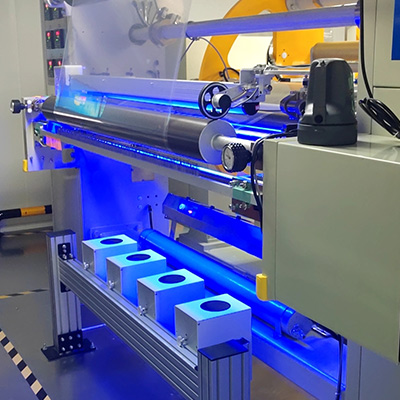
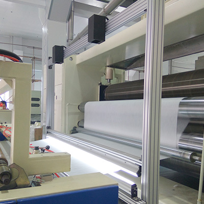
2.1 Machine Vision with Polarized Imaging and Multi-Spectral Analysis
Hardware Configuration:
Line-Scan Cameras with Ultra-High Resolution: 12k+ pixel line sensors capture full-width PI film images at speeds matching 800 m/min production lines, enabling 5-micron pixel resolution.
Circular Polarization Setup: Eliminates specular reflections from the film's smooth surface, enhancing visibility of low-contrast defects like faint scratches or coating thickness variations.
Multi-Spectral Illumination: Combines UV (254 nm for contamination detection), visible (525 nm for color anomalies), and NIR (850 nm for sub-surface delamination) to detect defects across material layers.
Image Processing Pipelines:
Phase Congruency Analysis: Identifies edges and textures invariant to lighting changes, critical for detecting scratches on uniform PI surfaces.
Anisotropic Diffusion Filtering: Reduces noise while preserving defect contours, improving accuracy for pinhole detection in ultra-thin films.
Defect Morphology Classification: Algorithms categorize defects by shape (e.g., linear scratches vs. circular particles) using Zernike moments or Hu invariants.
Case Study: A flexible PCB manufacturer achieved 99.97% detection accuracy for 10-micron pinholes using a line-scan system with polarized backlighting, reducing product failures in automotive displays by 90%.
2.2 Deep Learning for Rare and Complex Defects
Given PI film's low defect occurrence rate and high dimensional variability, deep neural networks (DNNs) offer transformative solutions:
Few-Shot Learning Models:
Meta-Learners (e.g., MAML): Train on minimal labeled defect samples (as few as 5 examples per class) by leveraging prior knowledge from generic material datasets, addressing the scarcity of real-world PI defect images.
Synthetic Data Generation via GANs: Generate realistic defects (e.g., simulated particle contamination or stress-induced micro-cracks) by conditioning GANs on PI film texture statistics, augmenting training datasets by 500%.
Hybrid CNN-LSTM Architectures:Process sequential film images to detect periodic defects (e.g., roller-induced scratches repeating every meter) by combining spatial feature extraction (CNN) with temporal pattern analysis (LSTM).
Technical Breakthrough: A custom U-Net model with attention mechanisms achieved 99.1% IoU (Intersection over Union) for wrinkle segmentation in curved PI substrates, outperforming traditional vision by 35% in complex geometries.
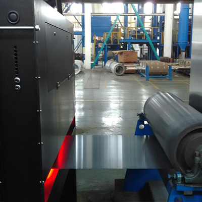
2.3 Non-Visual Sensing for Sub-Surface and Thermal Defects
Complementary to visual inspection, non-visual techniques address hidden flaws:
Laser Scanning Profilometry:Maps 3D surface topography with 1-micron height resolution to detect micro-wrinkles (height variation>5 microns) or thickness 不均 (e.g., 2% local thinning in aerospace-grade PI films).
Infrared Thermography:Detects thermal conductivity anomalies caused by delamination or voids in multi-layer PI composites, critical for insulating components in aircraft engines.
Atomic Force Microscopy (AFM):Provides nanoscale surface roughness analysis for ultra-precision applications (e.g., PI films used in MEMS sensors), though limited to offline 抽检.
3. Industry-Specific Applications and Quality Assurance
3.1 Flexible Electronics Manufacturing
OLED Display Substrates:Automated optical inspection (AOI) systems detect 5-micron-sized foreign particles that could cause display dark spots, ensuring yield rates >98% for 8K resolution panels.
Flexible PCBs:Deep learning models identify hairline cracks in PI-based circuit traces, preventing intermittent electrical failures in foldable smartphones. A leading OEM reduced rework costs by $2M annually through early defect detection.
3.2 Aerospace and Defense
Thermal Insulation Films:Combined vision-IR systems inspect PI films for both surface contamination (e.g., metal filings) and sub-surface voids, ensuring compliance with FAA flammability standards (e.g., FAR 25.853).
Satellite Solar Arrays:Laser profilometry verifies surface flatness of PI-based solar concentrator films, critical for maintaining optical efficiency in harsh space environments.
3.3 High-Temperature Industrial Processes
Fuel Cell Separators:Detection of oxidation-induced discoloration on PI-coated bipolar plates, preventing performance degradation in hydrogen fuel cells operating at 150°C.
4. Challenges and Future Innovations
4.1 Current Limitations
High-Temperature Imaging: Existing cameras struggle with motion blur at 300°C+ during continuous production; developing thermal-stable optical components is a priority.
Multi-Layer Defect Penetration: Sub-surface defects in laminated PI films (e.g., PI/copper composites) require deeper imaging penetration, pushing the limits of visible-light systems.
Real-Time Data Processing: Managing 10GB+/minute image data from high-speed lines demands edge computing solutions with embedded FPGA/GPU acceleration.
4.2 Future Directions
Self-Optimizing Inspection Systems:AI-driven auto-adjustment of lighting angles, camera exposure, and algorithm parameters based on real-time film properties (e.g., transparency, thickness), reducing manual calibration by 80%.
Quantum Machine Vision:Exploring quantum image sensors for enhanced sensitivity in low-light conditions, potentially enabling single-photon detection of ultra-small defects.
Digital Twin-Driven Detection:Virtual models simulate PI film formation processes to predict defect-prone zones, allowing proactive process control (e.g., adjusting roller pressure to prevent wrinkles).

Surface defect detection in PI films is a critical enabler for advanced technologies, requiring a fusion of cutting-edge imaging, machine learning, and material-specific sensing. As applications demand thinner, more complex PI structures—from foldable electronics to next-gen aerospace composites—the integration of adaptive AI, multi-modal sensing, and real-time analytics will be indispensable. These technologies not only ensure product reliability but also drive innovation by unlocking new design possibilities for high-performance PI-based materials. In an era where micron-scale precision defines competitive advantage, automated defect detection stands as the cornerstone of PI film manufacturing excellence.


 Top
Top
 Email
Email
 WhatsApp

 Submit Form
 Down
Down